Controlling 8 LEDs Using SN74HC595 Shift Register
HARDWARE REQUIRED:
- PICUNO Microcontroller board
- 8 × LEDs
- 8 × 220Ω resistors
- 1 × SN74HC595 Shift Register
- Breadboard
- Jumper wires
- USB cable
DESCRIPTION:
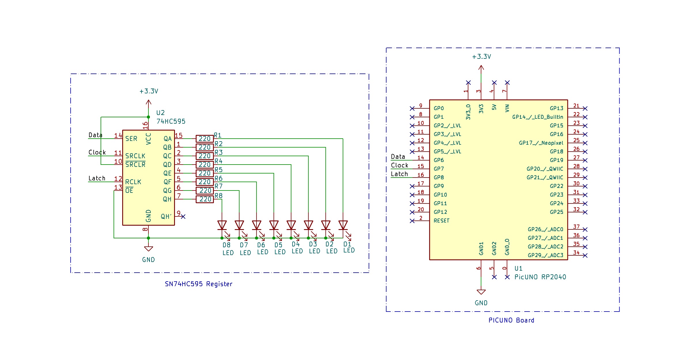
The SN74HC595 shift register allows you to control 8 LEDs using only 3 GPIO pins from the PicUNO. This is achieved by sending a serial stream of bits (representing LED states) to the shift register, which then latches and outputs them simultaneously on its 8 parallel output pins (Q0--Q7).
CIRCUIT DIAGRAM:
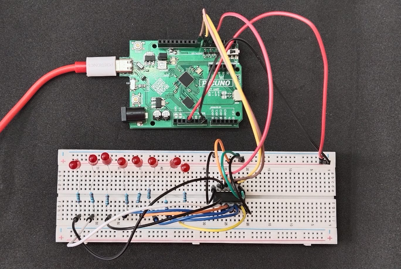
- Connect the PICUNO board to the computer using a USB cable.
- Connect the SN74HC595 Pins 1 -- 7, 15 to 8×220Ω resistors where each of them is connected to the anode of 8 LEDs.
- Connect the cathode of all LEDs to GND.
- Connect Pins 8 and 13 to GND.
- Connect Pins 10 and 16 to 3.3 V.
- Connect Pins 11, 12, 14 to GPIO 7, 8, 6 respectively.
SCHEMATIC:
SN74HC595 Pin 1--7, 15 (Q0--Q7) → 8x 220-ohm resistors → LEDs anode
LEDs cathode → GND
Pin 8 → GND
Pin 16 → VCC (3.3 V)
Pin 10 (MR) → Connect to VCC (keep shift register active)
Pin 13 (OE) → Connect to GND (output enable active)
Pin 11 (SRCLK/Clock) → Connect to GPIO 7
Pin 12 (RCLK/Latch) → Connect to GPIO 8
Pin 14 (SER/Data) → Connect to GPIO 6
CODE -- C:
int dataPin = 6; // SER
int clockPin = 7; // SRCLK
int latchPin = 8; // RCLK
void setup() {
pinMode(dataPin, OUTPUT);
pinMode(clockPin, OUTPUT);
pinMode(latchPin, OUTPUT);
}
void loop() {
for (int i = 0; i < 8; i++) {
byte value = 1 << i; // Shift a 1 through 8 positions
digitalWrite(latchPin, LOW);
shiftOut(dataPin, clockPin, MSBFIRST, value);
digitalWrite(latchPin, HIGH);
delay(200);
}
}
shiftOut() - Sends data serially, MSB first, to the shift register.
1 << i - Creates values like 00000001, 00000010, ..., shifting a single HIGH through bits.
latchPin LOW -> shiftOut -> latchPin HIGH - This sequence updates the outputs.
1 << i - Creates values like 00000001, 00000010, ..., shifting a single HIGH through bits.
latchPin LOW -> shiftOut -> latchPin HIGH - This sequence updates the outputs.
CODE -- PYTHON:
from machine import Pin
import time
dataPin = Pin(6, Pin.OUT)
clockPin = Pin(7, Pin.OUT)
latchPin = Pin(8, Pin.OUT)
def shiftOut(value):
for i in range(7, -1, -1): # MSB first
bit = (value >> i) & 1
dataPin.value(bit)
clockPin.value(1)
time.sleep_us(1)
clockPin.value(0)
while True:
for i in range(8):
value = 1 << i
latchPin.value(0)
shiftOut(value)
latchPin.value(1)
time.sleep(0.2)
shiftOut(value) - Manually sends each bit from MSB to LSB.
dataPin.value(bit) - Sets data line.
clockPin.value(1) - Pulses the clock to shift in the bit.
latchPin.value(1) - Updates all outputs at once after byte sent.
1 << i - Generates a pattern where one LED turns ON at a time.
dataPin.value(bit) - Sets data line.
clockPin.value(1) - Pulses the clock to shift in the bit.
latchPin.value(1) - Updates all outputs at once after byte sent.
1 << i - Generates a pattern where one LED turns ON at a time.